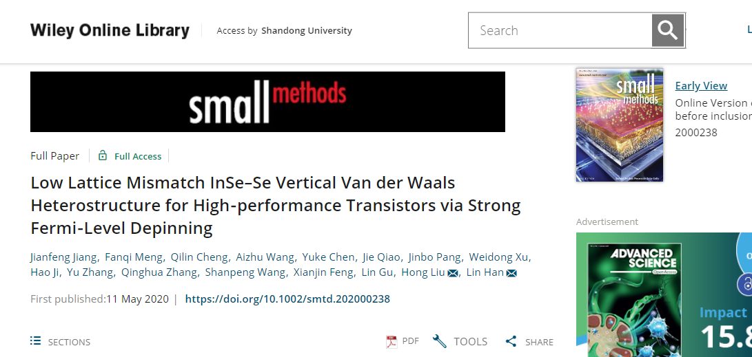
Recently, Prof. Han Lin’s in Institue of Marine Science and Technology has achieved new progress in low lattice mismatch (1.1%) InSe-Se heterostructure devices, whichprovides a highly valuable strategy to improve the contact condition of metal/2D semiconductors for high-performance, 2D-based electronics and optoelectronics. This result---“Low Lattice Mismatch InSe–Se Vertical Van der WaalsHeterostructure for High-performance Transistors viaStrong Fermi-Level Depinning” was published as cover article in the journal《Small Method》(Real-time IF: 12.5).Prof. Han Lin and Prof. Liu Hong are the corresponding authors, and Shandong University is the independent corresponding organization. Jiang Jianfeng, Meng Fanqi, Cheng Qilin and Wang Aizhu are co-first authors.
The difficulty in creating excellent contacts between metal/semiconductors for 2D-based devices limits exploration of the fundamental properties of 2D materials and hinders fabrication of high-performance electronic devices especially in low-operation voltage regimes and short-channel devices. Theoretically, it is predicted that a much lower contact resistance in 2D-based devices might be achieved compared to previously reported experimental values, with the related study still in its infancy. Therefore, optimizing the contact condition for metal and 2Dsemiconductors is an important technological challenge.The main challenge in creating contacts is Fermi-level pinning due to unintentional doping and damage at the metal-semiconductor interface in direct metallization, and the adsorbed contaminants (adsorbed water or hydrocarbon layers on the surface) which are incorporated at the contact interface. This leads to the creation of interface states that can pin the Fermi-level and increase the contact resistance. As a result, a facile and effective method for improving metal-2D semiconductor contacts is desired for high-performance 2D-based devices.
To address the above issues,Han’s groupreports that the formidable challenges mentioned above can be conquered efficiently via alow lattice mismatch (1.1%, through density functional theory (DFT))InSe-Se vertical vdW heterojunction to improve the contact condition, which is a facile and effective strategy that does not involve direct chemical bonding at the 2D-InSe surface.The Se layers not only prevent InSe from being damaged in direct metallization but also act as an ultrathin encapsulation layer to improve device stability. The InSe-Se heterojunction devices exhibit a high field-effect mobility of ~2500 cm2/V·s, an excellent on-state current of 1 mA, a threshold voltage of -0.7 V, and a hysteresis as low as 1.4 V. The time-dependent electrical stability was systematically analyzed. The field-effect mobilityexhibits a negligible change of 3.46% over two months of exposure to the ambient. Furthermore, the InSe-Se heterojunction devices exhibit a photoresponsivity time ~50% shorter than that of InSe devices in practical application, andhave a broad wavelength response range. This strategy is a valuable approach that can be easily expanded to other 2D semiconductors and opens up new opportunities for building high-performance 2D-based electronics and optoelectronics.
In the past two years, Prof. Han Lin and her research team have made a series of advances in the fields of new electronic material devices, biomedical engineering and their frontier interdisciplinary applications, such as: Low power nitrogen plasma for rapid repair of intrinsic defects in high-performance binary electronic devices (Small, 2019, 1901791. Cover article, IF: 10.856), single-cell analysis based on microfluidic technology (Small, 2019, 1905001. Cover article, IF:10.856), new electronic devices with high stability for real-time in-situ detection of neural signals (npj 2D Materials and Applications, 2019, 3, 29. Nature partner journal, 2019 real-time predictive impact factor 7.5-10), and highly sensitive two-dimensional pressure sensors based on piezoelectric effects (Nano Energy, 2020, 70, 1044457.IF: 15.548). Relevant work has been reported many times by academic media such as Materials Views China and Materials people, and cited and reported many times by authoritative journals in the field, such as Chem. Rev. Adv. Func. Mater. Research(AAAS).
This research was supported by the National Key R&D Plan of China, Natural Science Foundation for Yung Scientists of China, Natural Science Foundation for Distinguished Young Scientist of Shandong Province, the Key Research Program of Frontier Sciences, CAS, the Shandong University Multi-Disciplinary Research Grant, the National Natural Science Foundation of China and the Natural Science Foundation of Shandong Province. The computational resources were provided by the Centre for Advanced 2D Materials of the National University of Singapore in Singapore. We thank the support from the Collaborative Innovation Center of Technology and Equipment for Biological Diagnosis and Therapy in Universities of Shandong.
The link to:https://onlinelibrary.wiley.com/doi/10.1002/smtd.202000238
https://onlinelibrary.wiley.com/doi/10.1002/smll.201901791
https://onlinelibrary.wiley.com/doi/abs/10.1002/smll.201970279
https://www.nature.com/articles/s41699-019-0110-x
https://www.sciencedirect.com/science/article/abs/pii/S2211285520300136
Written by:Han Lin
Edited by: Che Huiqing